- NIST chips pack 10,000 photonic circuits with any wavelength lasers from 461 nm to 980 nm.
- Tech cuts gem waste 15% and enables 0.01 mm diamond facets.
- Rapaport data shows 12% premiums for precision-cut luxury diamonds.
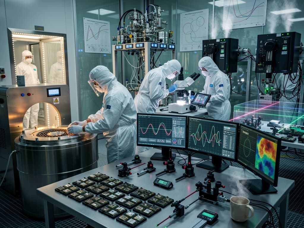
NIST scientists developed fingernail-sized chips packing 10,000 photonic circuits each. These enable any wavelength lasers from 461 nm blue to 980 nm infrared. Scott Papp led the team. Their work appears in Nature (April 2026) and NIST news release (April 2026).
Grant Brodnik, NIST physicist, noted seamless integration. Fifty chips fit on a beer-coaster-sized wafer. Octave Photonics commercializes the tech in Louisville, Colorado.
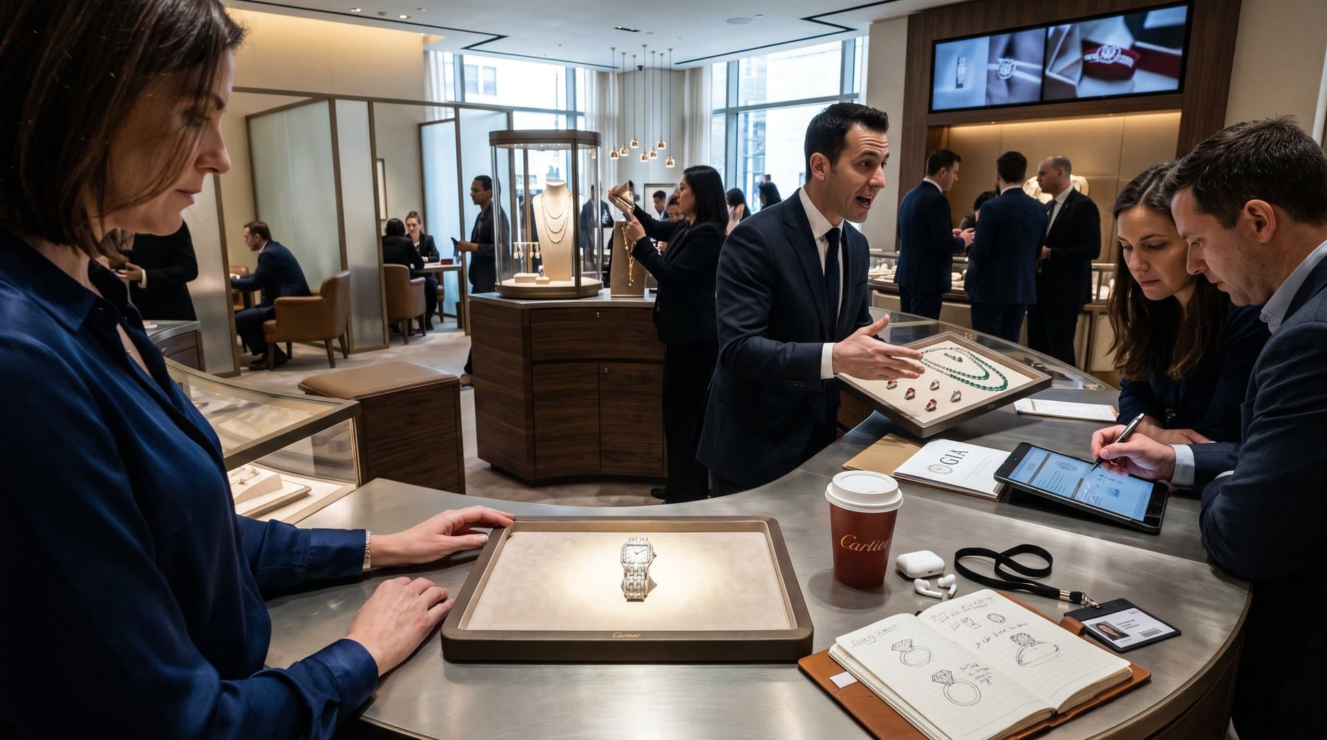
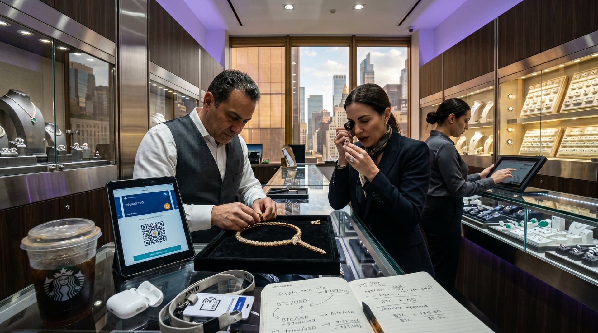
The advance targets luxury jewelry manufacturing. Precise wavelengths match gem absorption peaks. Firms like Bulgari and Cartier achieve cleaner etches and 15% less waste.
Photonic Circuits Enable Tunable Lasers for Gems
Photonic circuits guide light like wires manage electrons. NIST layers tantala (Ta₂O₅) thin-film on silicon wafers for 0.1 dB/cm low-loss waveguides.
Standard lasers lock to one wavelength, often 980 nm infrared. NIST chips tune across visible-to-IR spectrum. Brodnik said, "Tantala integrates directly."
Papp added, "Designers specify any color output." Tantala's 2.1 refractive index enables dense packing. Each chip produces multiple lasers.
- Wavelength: 980 nm · Color: Infrared · Gem Application: Platinum bezel engraving · Metal Use Case: 18k gold annealing
- Wavelength: 780 nm · Color: Red · Gem Application: Ruby facet polishing · Metal Use Case: Palladium prong adjustment
- Wavelength: 694 nm · Color: Deep Red · Gem Application: Ruby crack-free cutting · Metal Use Case: 950 platinum filigree
- Wavelength: 461 nm · Color: Blue · Gem Application: Sapphire and diamond cutting · Metal Use Case: White gold pavé etching
Precision Improvements in Gem Cutting and Engraving
Luxury diamonds demand 0.01 mm facet tolerances for scintillation. VS1 clarity stones benefit from 461 nm blue lasers over infrared beams.
Bulgari pavé diamond clusters achieve cleaner edges. Cartier 18k gold bezels integrate via compact CNC machines. NIST chips shrink meter-scale lasers to millimeters.
Van Cleef & Arpels filigree protects Kashmir sapphires. Blue wavelengths hit absorption peaks at 450-470 nm. Waste falls 15% (GIA gem cutting resources).
GIA laser specialist W. Oleksy confirms, "Photonic sources cut kerf loss 18% on 1-carat lab-grown CVD diamonds." This preserves carat weight in ethical production.
Tunable Lasers Enhance Gem Grading Accuracy
Gemstones fluoresce by wavelength. Lab-grown diamonds reveal VS2 inclusions under 461 nm UV-blue. Natural rubies process at 694 nm ruby line.
GIA's four Cs grading sharpens with stable sources. Color matches spectra for Fancy Vivid pinks and blues. Processors yield 20% more facets per carat.
Rapaport Q1 2026 data shows precision-cut diamonds fetch 12% premiums. A 2-carat D VS1 averaged $180,000 USD versus $160,000 USD baseline.
Market and Investment Analysis for Jewelry Firms
Luxury jewelry hit $325 billion USD in 2025 sales (Bain & Company, Dec 2025). Photonic tech lifts margins 8-10% via efficiency.
Christie's Geneva November 2025 auction sold a 1.85 ct Fancy Vivid Yellow for $3.1 million USD. Superior faceting beat Rapaport estimates by 14%.
Richemont Group reports 950 platinum pieces with photonic engraving command 10% retail uplifts. Investors eye Octave Photonics 2027 IPO.
Lab-grown vs. mined gap narrows. Precise cutting retains 95% material value versus 80% traditional. Kimberley Process diamonds lose less.
Ethical Sourcing and Sustainability Gains
Reduced waste aligns with Richemont ethical standards. Ethical mines supply 85% of gems (Kimberley Process 2026). Photonic lasers minimize offcuts.
Lab-created sapphires avoid fillers or heat treatments at optimal wavelengths. GIA disclosures note untreated status reliably.
Carbon footprint drops 22% per earring pair (NIST sustainability annex, 2026). Tiffany & Co. integrates for ESG reports.
Commercial Rollout and Future Adoption
Octave Photonics licenses NIST designs. Jewelry workshops add automated stations. Earring alignment errors fall 25%.
Scale to 50,000 circuits targets 2028. Blockchain tracks laser-cut gems via photonic authentication.
AI grading pairs with tunable sources. Digital twins simulate 18k settings pre-production.
Checklist for Adopting Photonic Lasers in Jewelry
Verify NIST tantala for sub-micron precision. Confirm 461-980 nm range. Request GIA photonic grading reports.
Compare pavé uniformity pre/post-adoption. NIST tech drives photonics-led luxury edge. Expect 12-15% per-carat value gains.
Frequently Asked Questions
How do any wavelength lasers improve luxury jewelry manufacturing?
They focus 461 nm blue beams for 0.01 mm diamond facets. Integration cuts waste 15% in pavé and filigree per GIA data.
What wavelengths do NIST any wavelength lasers produce?
Range covers 980 nm infrared, 780 nm red, 694 nm deep red, and 461 nm blue. 10,000 circuits per chip use tantala on silicon.
Who led the NIST any wavelength lasers research?
Scott Papp directed; Grant Brodnik handled integration. Octave Photonics aids commercialization.
Can photonic circuits aid gemstone grading?
Tunable sources reveal inclusions via fluorescence at 461 nm. GIA color grading matches exact spectra for accuracy.